

Scanning Tunneling Microscopes STM
STM
Quazar Tech provides a range of cutting-edge Scanning Tunneling Microscopes (STMs) designed for imaging conductive surfaces at extremely high magnifications—down to the scale of individual atoms. These powerful instruments allow researchers and experts in the field of probe microscopy to explore the fascinating nano-world with ease. Whether you’re a beginner or an experienced scientist, Quazar’s STMs offer a superb combination of sophistication and user-friendliness.
In addition to the STMs, Quazar Tech also supplies widely used STM samples and essential accessories. Whether you’re conducting groundbreaking research or educational experiments, Quazar’s STMs empower you to explore the nanoscale world with precision and confidence.
Scanning Tunneling Microscopes : Product Group Stats
Scanning Tunneling Microscopes : Products & Solutions
Products
nanoREV™ Air STM
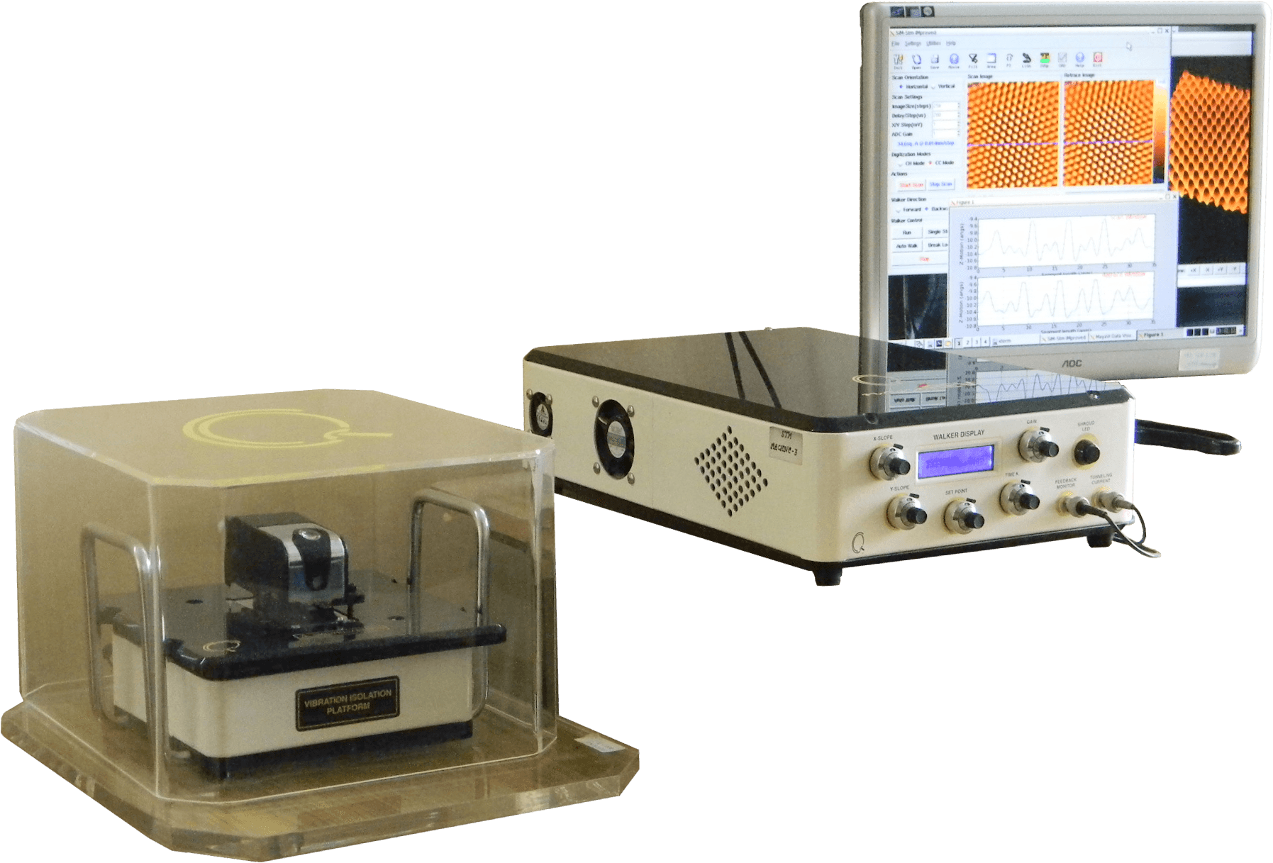
The nanoREV™ Air STM is an ambient air STM which opens out the fascinating nano-world right on to your table-top. It comes with a superb combination of ease-of-use and a high-level of sophistication, making it a ready-to-use instrument both for the beginners and the experts in the field of probe microscopy.
nanoREV™ Vacuum STM
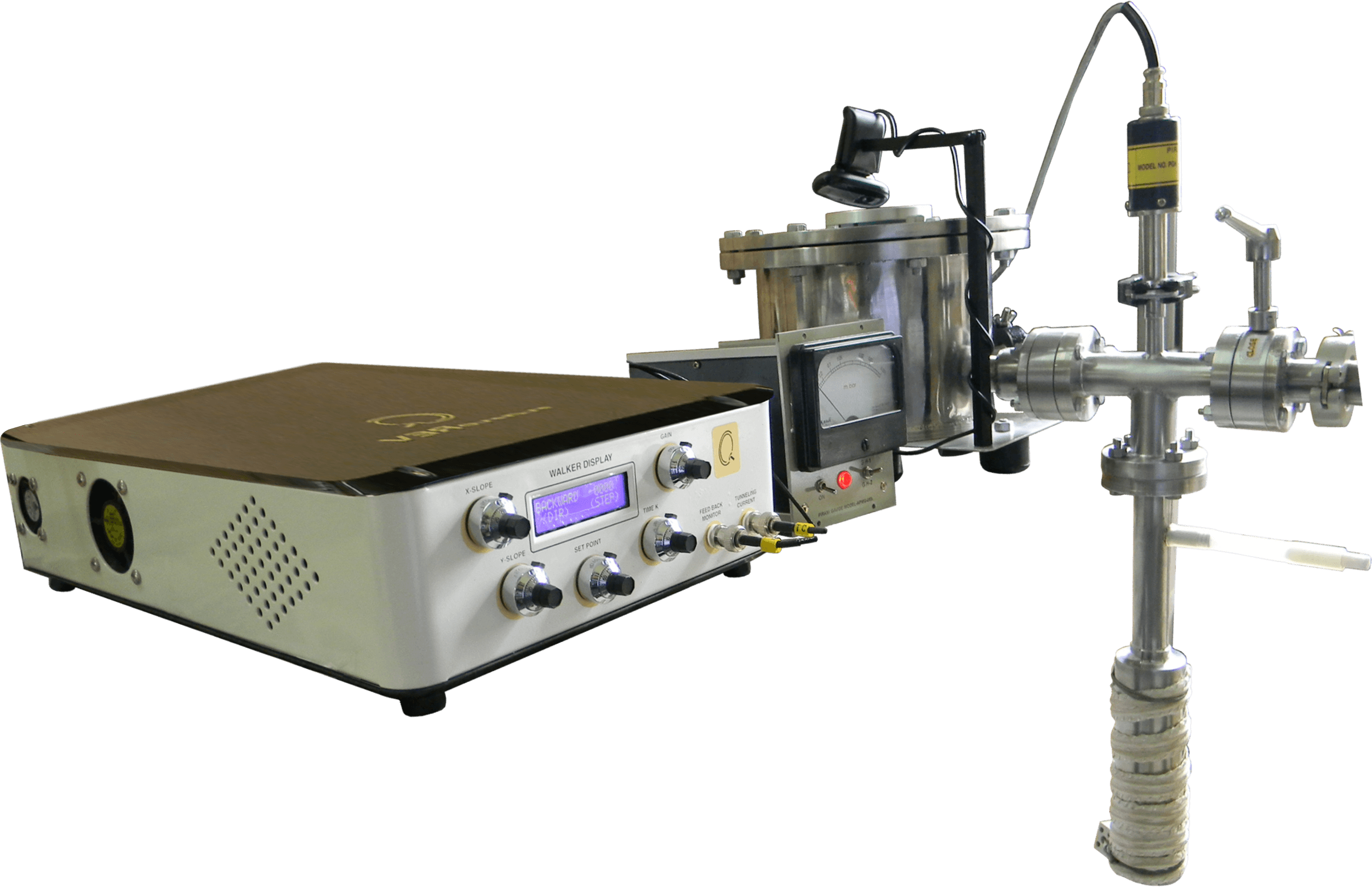
The nanoREV™ Vacuum STM operates with the scan head and the sample contained in a vacuum environment, spanning from ambient conditions down to 10^-3 mbar. Its vibration-free pumping system utilizes a sorption pump immersed in liquid nitrogen. It features a compact chamber footprint (just 25 cm in diameter) and has a viewing window for the tip-sample junction. All vibration isolation components are contained within the chamber.
nanoREV™ Low Temperature STM
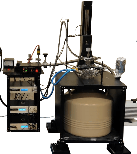
The nanoREV™ LT-STM facilitates precise surface imaging across a temperature range of 77K to 330K. Its automated hoisting mechanism and rotary scan-head streamline ex-situ tip and sample replacements, making the process as straightforward as working with an ambient STM.
Accessories

Lock-In Amplifier
STM Lock-In Amplifier
Fine tuned for use with the STM, the SLIA lock-in amplifier enables LDOS and LBH mode imaging in the nanoREV STMs.

Tip Fabrication Unit
nanoETCH™
The quality of images obtained using an STM is critically dependent on the nature of the probing tip. The nanoETCH unit is used for the preparation of tungsten tips by an electro-chemical etching process.
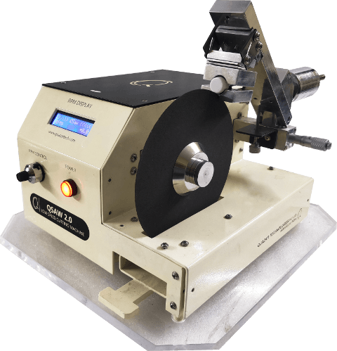
Low Speed Cutting Machine
QSAW
Useful for sectioning/shaping hard and brittle samples into appropriate dimensions suitable for characterization sample-stages.
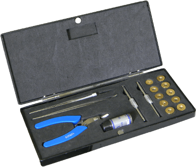
nanoREV™ STM Toolkit
Included with every nanoREV™ STM, this toolkit includes all the tools and consumables you need to get started with the STM.
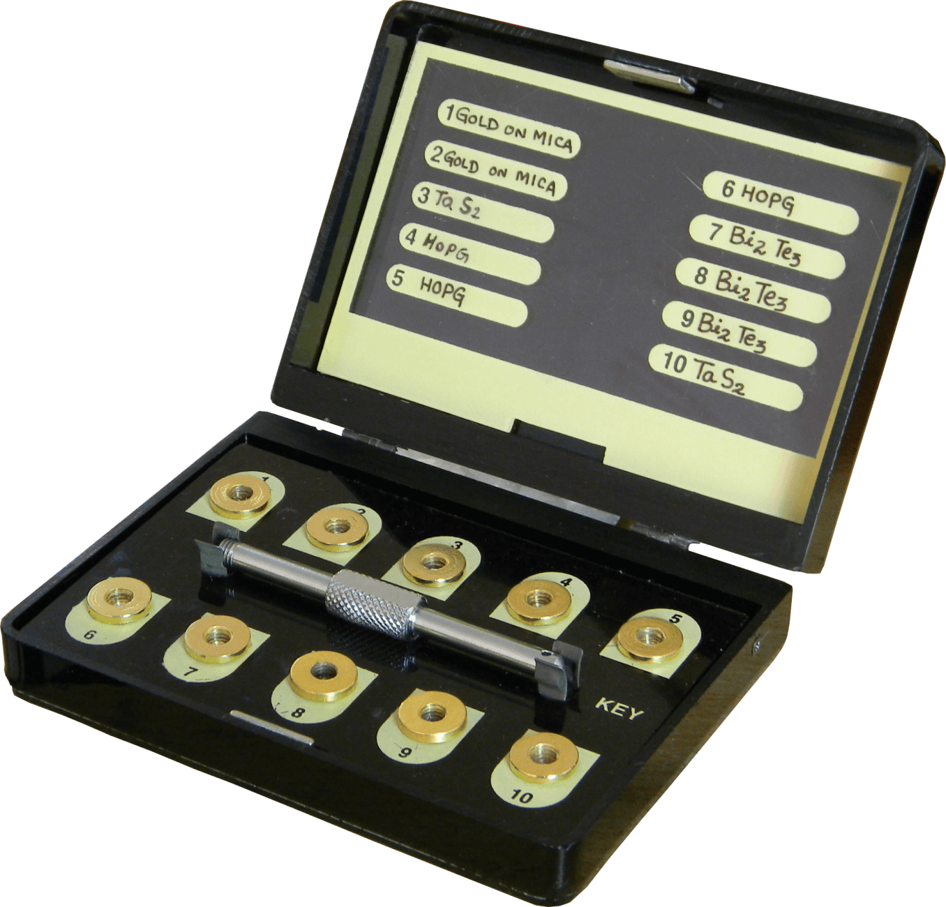
nanoREV™ STM Sample Library
Thoughtfully curated samples for the SPM user community, complete with pre-mounted sample discs for seamless loading and instant utilization. Compatible with the nanoREV Air and Vacuum STMs. Ideal for training, educational labs, and validation.
Consumables
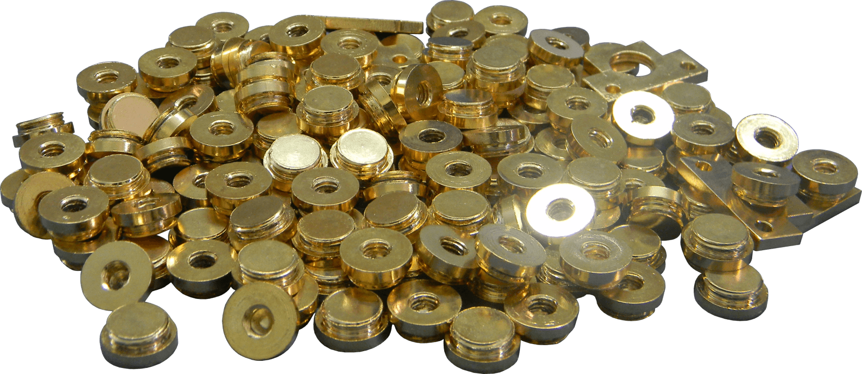
Sample Mounting Discs for nanoREV™ STMs
Threaded electroplated MS discs of 10 mm diameter for mounting samples. Compatible with the nanoREV™ Air and Vacuum STMs. [check for LTSTM]
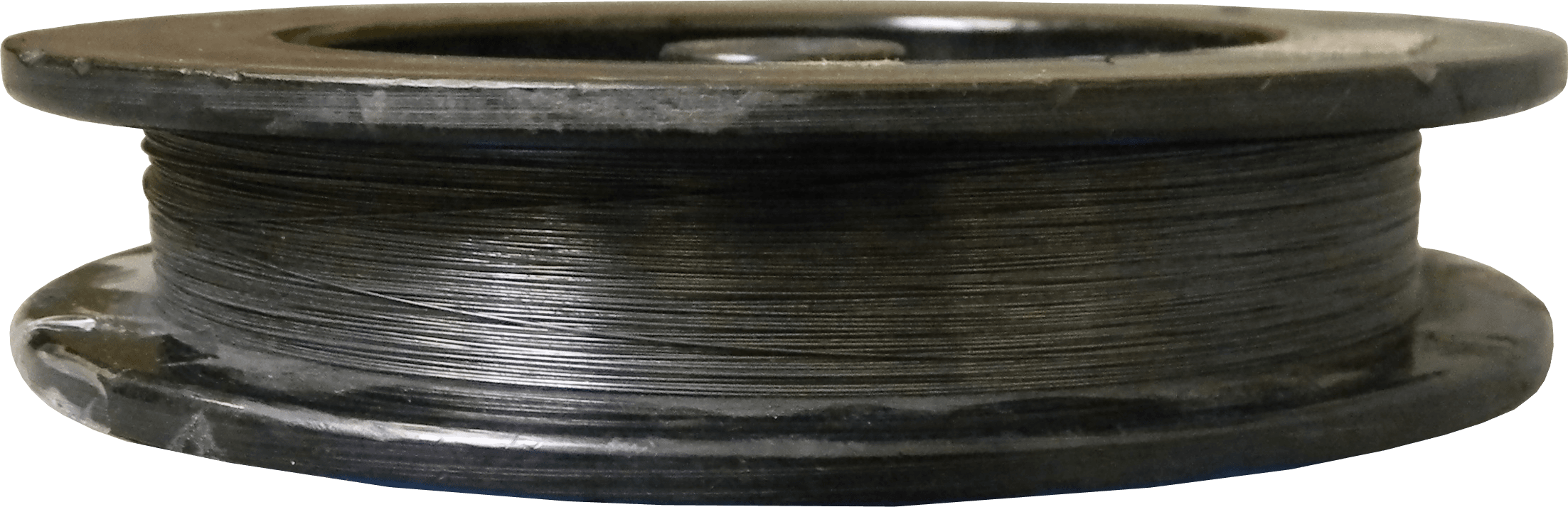
Tip Wire for nanoREV™ STMs
Wire suitable for STM tips. Compatible with all nanoREV STMs. Both Pt/IR and Tungsten wire are available.

Conducting Silver Ink
Conductive Silver Ink is used to establish electrically conductive contacts on samples in a non-destructive manner.
nanoREV™ STM Scans Exploring the Nanoscale World
Exploring the Nanoscale World
Explore the captivating allure of the nanoscale realm with our nanoREV STMs. Delve into intricate patterns, atomic landscapes, and quantum marvels, all meticulously captured with our state-of-the-art technology.
Whether you’re a scientist, educator, or simply curious, we invite you to appreciate the elegance and complexity of the nanoscale. Each scan tells a story of atoms, bonds, and forces - a testament to human curiosity and the continuing march of technology and science, hand in hand, deeper into the hidden realities of the universe we inhabit.
Showing images with tags :
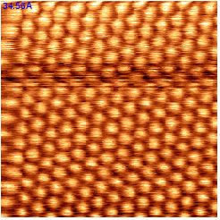
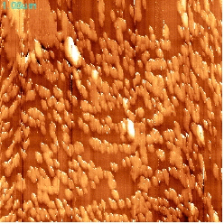
An atomic resolution scan of Highly Ordered Pyrolytic Graphite (HOPG) taken using Quazar Tech's nanoREV STM
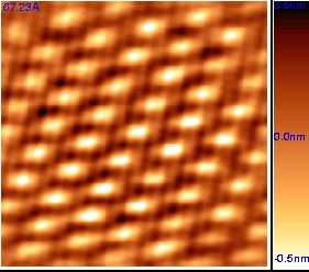
In this large area STM scan (43 nm × 43 nm), superstructures arising from Moiré patterns among the layers of HOPG. These patterns emerge from interference effects caused by misalignments between periodic lattices or layers thereof. The interference leads to variations in electron density, resulting in the visually striking patterns we see.
This atomic resolution STM scan of 1T-TaS2 shows the formation of charge density waves on the surface layer
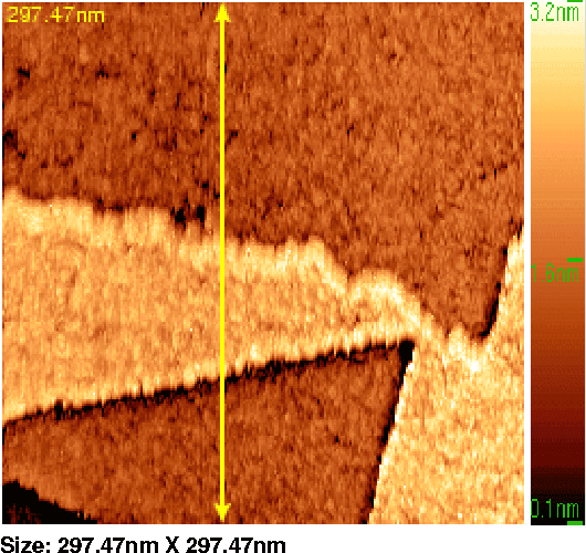
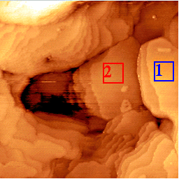
This 298nm x 298nm scan of a single crystal of Bismuth Telluride shows the layered structure of the material
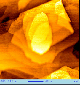
This sequence of STM scans of a Bismuth Telluride sample shows the extensive range of the nanoREV STM. Starting from a large area view of the surface grain structure, each subsequent image is a higher magnification level until we reach atomic resolution.
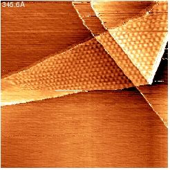
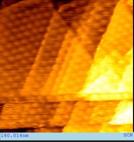
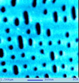
Terraces of Gold (Au) on Mica are seen in this 85nm x 85nm STM scan of a sample formed by thermal deposition followed by annealing.
This scan shows a multilayer graphene structure, with atomic resolution simultaneously observed at different layers
This sequence of STM scans is of a sample of Graphene deposited on a Copper substrate using Quazar's CVD. Starting from a large area view of the grown Graphene flakes, each subsequent image is a higher magnification level until we reach atomic resolution.
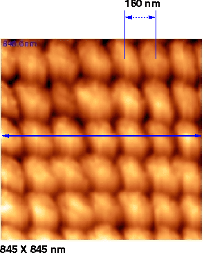
This expansive 845 nm × 845 nm image of a nano grid showcases the impressive field of view achievable with the nanoREV STM. Notably, the same instrument that captured this image is also capable of achieving atomic-scale resolution.
This STM scan of a Blu-ray disc reveals intricate surface structures and patterns. It allows us to visualize the arrangement of pits and lands—the fundamental features responsible for storing digital information on the disc.
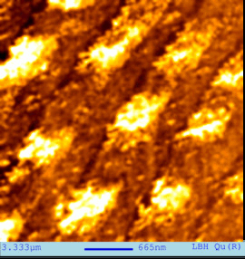
Captured using the powerful Local Barrier Height (LBH) mode of the STM, this scan of a DVD-RW vividly reveals the intricate bit patterns within the tracks. Unlike the simple topography scan, the LBH mode provides extraordinary detail about the local electronic properties of the material by measuring the energy barrier for tunneling.
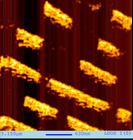
Captured using the powerful Local Density of States (LDOS) mode of the STM, this scan of a DVD-RW vividly reveals the intricate bit patterns within the tracks. Unlike the topology scan, the LDOS mode provides extraordinary detail about the local electronic properties of the material by measuring the available electronic states at each location.
If you'd like to contribute your scans with Quazar Tech's nanoREV STMs for inclusion in this collection, get in touch with us!
Customer Sites with our Scanning Tunneling Microscopes

Peer Reviewed Publications using our Scanning Tunneling Microscopes
Effect of silver nanoparticles on electrical and magnetic properties of reduced graphene oxide
Prajwal Chettria
Ajay Tripathib
Archana Tiwaric
aDepartment of Physics, Salesian College, Siliguri
bDepartment of Physics, School of Physical Sciences, Sikkim University
cDepartment of Physics, Institute of Science, Banaras Hindu University
Synthesis of nanodiamonds using liquid-phase laser ablation of graphene and its application in resistive random access memory
Anna Thomas
M S Parvathy
K B Jinesh
Department of Physics, Indian Institute of Space-Science and Technology
Programmable electronic synapse and nonvolatile resistive switches using MoS₂ quantum dots
Anna Thomas
A N Resmi
Akash Ganguly
K B Jinesh
Department of Physics, Indian Institute of Space-Science and Technology
Influence of surfactants on the electronic properties of liquid-phase exfoliated graphene
Sheena S Sukumarana
Saurabh Tripathib
A N Resmib
K G Gopchandrana
K B Jineshb
aDepartment of Optoelectronics, University of Kerala
bDepartment of Physics, Indian Institute of Space-Science and Technology
Low power organic field effect transistors with copper phthalocyanine as active layer
Lekshmi Vijayana
Anna Thomasb
K Shreekrishna Kumara
K B Jineshb
aDepartment of Electronics, School of Technology and Applied Sciences, Mahatma Gandhi University
bDepartment of Physics, Indian Institute of Space-Science and Technology
Studies of Surface Electrical Properties of Al doped ZnO Nanorods by STM
Shaivalini Singha
Sumit Vyasb
Parthasarthi Chakrabartib
Si-Hyun Parka
aDepartment of Electronic Engineering, Yeungnam University
bDepartment of Electronics and Communication Engineering, Motilal Nehru National Institute of Technology
Anisotropic Phase Formation Induced Enhancement of Resistive Switching in Bio–based Imidazolium Ionic Liquid Crystals.
Renjith Sasia
K B Jineshb
Sudha J Devakia
aChemical Sciences and Technology Division, CSIR-National Institute for Interdisciplinary Science and Technology
bDepartment of Physics, Indian Institute of Space Science and Technology
Detecting sub-nanometer transverse vibrations on a piezo crystal oscillator surface, using time series tunneling current measurements
Dibya J Sivananda
Amit Banerjee
S S Banerjee
Department of Physics, Indian Institute of Technology Kanpur
P-channel thin film transistors using reduced graphene oxide
S Chakraborty
A N Resmi
P Renuka Devi
K B Jinesh
Department of Physics, Indian Institute of Space-Science and Technology
Single quantum dot rectifying diode with tunable threshold voltage
Gopal S Kenatha
Piyali Maityb
Yogesh Kumarc
Hemant Kumarc
Vinod K Gangward
Sandip Chaterjeed
Satyabrata Jitc
Anup K Ghoshb
Bhola N Pala
aSchool of Material Science and Technology, Indian Institute of Technology (Banaras Hindu University)
bDepartment of Physics, Banaras Hindu University
cDepartment of Electronics Engineering, Indian Institute of Technology (Banaras Hindu University)
dDepartment of Physics, Indian Institute of Technology (Banaras Hindu University)
Liquid phase exfoliated graphene for electronic applications
Sheena S Sukumarana
K B Jineshb
K G Gopchandrana
aDepartment of Optoelectronics, University of Kerala
bDepartment of Physics, Indian Institute of Space-Science and Technology
H₂O₂ sensing using HRP modified catalyst-free ZnO nanorods synthesized by RF sputtering
Amit Srivastavaa
Naresh Kumara
Priti Singhb
Sunil Kimar Singhb
aDepartment of Physics, Motilal Nehru National Institute of Technology
bDepartment of Biotechnology, Motilal Nehru National Institute of Technology
HRP modified pulse laser ablated ZnO nanostructure for H₂O₂ sensing
Amit Srivastava
Naresh Kumar
Department of Physics, Motilal Nehru National Institute of Technology
Gate controllable resistive random access memory devices using reduced graphene oxide
Preetam Hazra
A N Resmi
K B Jinesh
Indian Institute of Space Science and Technology
Structural, Optical and Electrical Properties of Synthesized ZnO Nanoparticles
Rakesh Saroha
A K Panwar
Department of Applied Physics, Delhi Technological University
Controlled Synthesis of Nitrogen-Doped Graphene from a Heteroatom Polymer and Its Mechanism of Formation
Titash Mondala
Anil K Bhowmickb
Ramanan Krishnamoortic
aDepartment of Chemistry, Indian Institute of Technology, Patna
bRubber Technology Center, Indian Institute of Technology Kharagpur
cDepartment of Chemical and Biomolecular Engineering, University of Houston
Stress Generation and Tailoring of Electronic Properties of Expanded Graphite by Click Chemistry
Titash Mondala
Anil K Bhowmicka
Ramanan Krishnamoortib
aDepartment of Chemistry, Indian Institute of Technology Patna
bDepartment of Chemical and Biomolecular Engineering, University of Houston
Butyl lithium assisted direct grafting of polyoligomeric silsesquioxane onto graphene
Titash Mondala
Anil K. Bhowmicka
Ramanan Krishnamoortib
aDepartment of Chemistry, Indian Institute of Technology Patna
bDepartment of Chemical and Biomolecular Engineering, University of Houston
Fabrication of single and coupled metallic nanocantilevers and their nanomechanical response at resonance
Amit Banerjee
S S Banerjee
Department of Physics, Indian Institute of Technology Kanpur
Temperature-dependent morphological evolution of clustered gold surface
Mukesh Kumar
Govind
Physics of Energy Harvesting Division, National Physical Laboratory (CSIR)
Formation of Gallium-induced nanostructures on single crystal HOPG surface
Jaspreet Sandhu
Amit Kumar Singh Chauhan
Govind
Physics of Energy Harvesting, National Physical Laboratory (CSIR)
If you've used this instument in your published work and would like your paper to be included here, get in touch with us!
Why list here?
- Enhanced Visibility: Having your published work listed here can significantly boost its visibility among the instrument's growing user community. Whether you’re seeking potential collaborators or aiming to encourage further research, this platform provides an excellent opportunity to showcase your work.
- Development Insights: By sharing information about what our users are doing with our products, we gain valuable insights. This knowledge helps us plan and enhance our development efforts. Even if you prefer not to include your research in the public list, we still encourage you to let us know about it.
Our Scanning Tunneling Microscopes in the Press
Nano-revelations by the Indigenous nanoREV 4.0 Air STM
April 2011
The Center for Knowledge Management of Nanoscience & Technology